Photonics Assembly Services
Advanced Assembly, Alignment and Packaging for Photonic Devices.
Advanced Assembly, Alignment and Packaging for Photonic Devices.
Bringing a photonic device to market is a complex journey, design precision, thermal stability, optical alignment, and reliability all have to work together seamlessly.
That’s where our photonics assembly services come in.
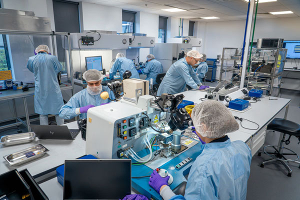
At Bay Photonics, we cover the full lifecycle of photonic packaging, from concept and prototype to full-scale production. We specialise in every stage of assembly and packaging with the flexibility, speed, and reliability your product demands.
How to Start your Photonic Project with Bay Photonics

Design & Develop
Work with our engineers to define your requirements and design a packaging solution tailored to your device.
You’ll gain a clear, manufacturable design that combines performance and reliability, right from the start.

Assembly & Integration
We assemble both standard and custom hermetic photonic packaging, combining die handling, pick and place, wire bonding, surface mount, optical coupling, and welding.
You’ll receive a precisely built package, fully integrated with thermal control, electronics, and optics, ready for testing and production.

Test & Validation
We conduct rigorous, industry-standard testing to ensure performance and reliability, including bond, shear, push, pull, leak, and environmental tests.
You’ll have complete confidence your device meets specification, passes qualification, and is ready for the market.
Design & Development
Collaborating with you from concept to manufacturing
Every successful photonic device starts with expert engineering. Our in-house design and development team works closely with you to define requirements, materials, and performance goals — covering optical, RF, mechanical, thermal, and environmental performance.
We offer high-reliability hermetic hybrid packaging and integration solutions, along with PIC design guidance, rapid prototyping, and design for volume manufacture.

Attach
We attach semiconductor dies to substrates or using solder, eutectic or epoxy materials suited to your thermal and mechanical needs. Our bonding solutions are precise, scalable, and production-ready, whether in a prototype or a production -grade LIDAR and optical communication modules.
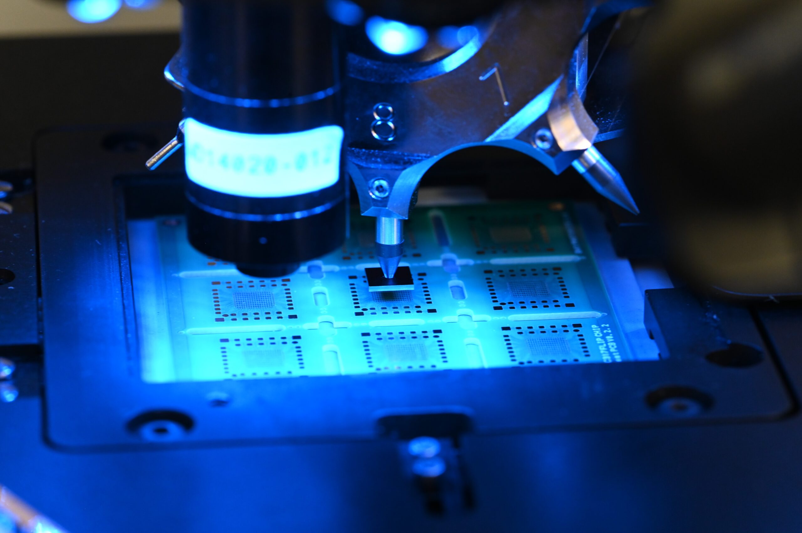
Die Bonding
Die bonding is a foundational process in the assembly of semiconductor photonic devices. Whether the application is a ladder emitter, LED, photodetector, or integrated optical sensor, the quality and precision of die attach impacts thermal management, optical alignment, and long-term reliability.
Solder, Eutectic & Epoxy Bonding
We offer a full suite of die attach technologies as we understand that different applications demand different strategies:
Solder attach for high thermal conductivity and mechanical strength.
Eutectic soldering for hermetic and high-reliability applications.
Wire Bonding
Devices are often compact, thermally sensitive, and require precise optical alignment - conditions where wire bonding offers unmatched flexibility. Our services support everything from early R&D through to production scale, combining gold and aluminum, dimensional precision (12-50 µm wires and ribbons) and engineering collaboration.
Vacuum
Vacuum capabilities ensure void-free soldering - essential for high-reliability or hermetically sealed packages.
We support a wide range of photonic device architectures including VCSELS, edge-emitters, photodiodes, and hybrid photonic integrated circuits (PICs). To create robust electrical connections between active and passive devices within your assembly we offer:
Ball Bonding
Ball bonding with gold wire provides robust electrical and thermal pathways for laser and detector applications.
Wedge Bonding
Wedge bonding with gold or aluminium allows for low-profile connections and excellent bond placement accuracy - dense optical packages or planar lead frames.
Ribbon Bonding
Ribbon bonding for applications requiring lower loop height, increased surface contact or specialised RF or high-current performance.
Key Capabilities
- Eutectic, solder or epoxy attach
- Gold and aluminum wire bonding
- Fully automated die bonding for volume manufacturing
- Semi-automatic die bonding supports rapid prototype builds and parameter optimisation
- X-ray tomography provides non-destructive quality assurance by detecting voids or bond defects
- Bonding capabilities ensure speed, precision and reliability.

Align & Integrate
Our optical alignment and integration services ensure precision coupling light into and out of edge-emitting lasers, photodetectors and photonic integrated circuits.
The quality of optical alignment and attach defines key parameters such as insertion loss, signal stability and system efficiency.
We use sub-micron alignment workstations to enable active and passive alignment of optical elements, supporting micro-optic alignment (lenses, isolators, filters), single fibre and fibre array alignment, edge-emitter and PIC alignment.
We integrate thermal control, electronics, and free-space or fibre optics into compact, high-performance photonic modules – delivering assemblies that are stable, efficient, and production-ready.
Key Capabilities
- Direct butt-coupling of single fibres or arrays to edge-emitting lasers and detectors, using index matching adhesive for low loss, high-stability joins.
- Free-space coupling from edge emitters into lensed fibres.
- Grating coupling alignment for coupling into silicon photonic PICs.
- Alignment processes combine precision motion stages with active alignment feedback (where applicable) to optimize optical throughput prior to cure or bonding.
- Optical attach methods - including UV adhesives, index-matching epoxies, low-outgassing options for sealed or vacuum environments.
- Automated and guided processes for repeatable coupling and fixative dispensing to ensure alignment integrity and maintaining flexibility.

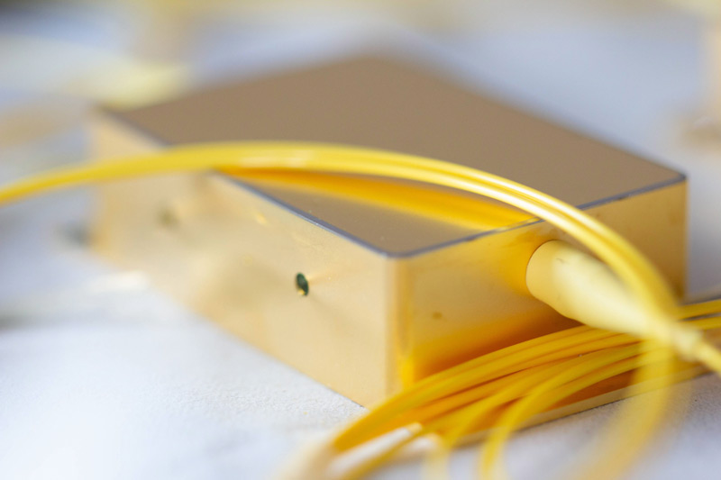
Seal the Deal – Hermetic Packaging
We protect your photonic devices with hermetic sealing techniques that guard against moisture, contamination, and mechanical stress.
Our capabilities include resistive seam welding and projection welding.
The packages we build:
TO cans
(Transistor outline) are metal can enclosures with a glass-to-metal seal for electrical feedthroughs and an optional lens or window for optical access. Used for laser diodes and photodiodes especially in telecoms.
Gold Boxes
Are rectangular or custom-shaped metal enclosures (kovar, plated in gold) housing complex photonic assemblies. These provide thermal and mechanical stability and can be precisely tailored to specific geometries. These enclosures incorporate TECs and Thermistors for precise temperature control and long-term stability in demanding environments.
Resistive welding
(seam welding) a lid is pressed onto the package flange and a controlled electrical current is passed through electrodes to generate heat via electrical resistance. The materials fuse in a continuous seam ensuring a strong and reliable weld without damaging the components inside.
Projection welding
involves tiny raised projection points on one of the surfaces being welded. When current is applied, these points heat and collapse, forming multiple localised welds at once. This is ideal for small packages and tight thermal budgets.
- Hermetic welding (resistive or projection).
- Custom metal or ceramic enclosures.
- Extended device lifetime and long-term reliability
- Proven protection for space, defence, telecom and quantum systems.
- Temperature and optical stability.
- Primary advantage of a TO Can is the ability to achieve true hermeticity.
Test & Validation
To ensure your devices perform as designed, we conduct mechanical, optical and environmental testing.
Our systems provide fine control of bonding parameters – force, ultrasonic energy, time and loop profile – with built in monitoring and in-process inspection. This includes bond, shear, push, and pull strength testing as well as hermetic leak and environmental qualification to Telcordia and MIL-STD standards.
We deliver photonics assembly services for industries where reliability is mission-critical, including telecom, quantum, defence, medical, and space applications.
Each solution is tailored to meet your performance and compliance standards, giving you the confidence to scale with precision.
Key Capabilities
-
Die shear strength to
MIL-STD-833-2 method 2019.10 -
BGA ball shear testing to
JEDEC JESD22-B117B -
Wire bond pull test to
MIL-STD-883-2 method 2011.10 -
Fine leak and gross leak
hermeticity seal test and validation
to MIL-STD-883-1 method 1014.17
-
Residual internal gas analysis to
MIL-STD-883-1 method 1018.6 -
Optical and electrical
performance verification -
Confidence in product
reliability and compliance - From design for assembly to final test - this accelerates product development while reducing risk

We deliver photonics assembly services for industries where reliability is mission-critical, including telecom, quantum, defence, medical, and space applications.
Each solution is tailored to meet your performance and compliance standards, giving you the confidence to scale with precision.

Ready to discuss your Photonics Packaging needs?
Let’s bring your idea to life.